
Currently Empty: ₹0.00
Product Description
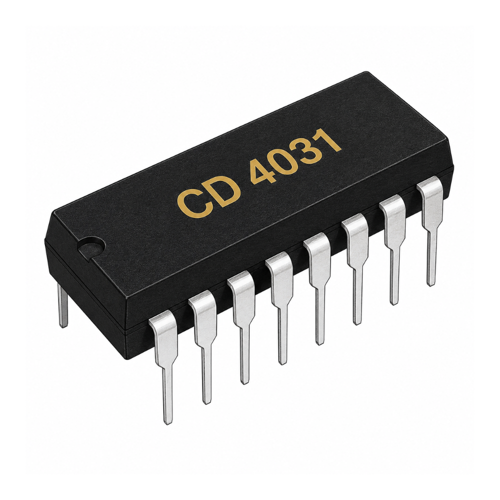
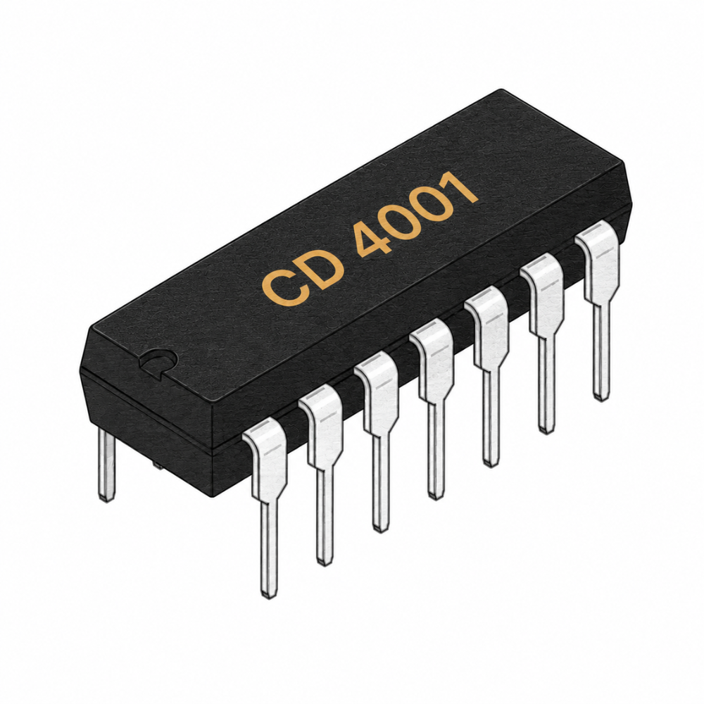
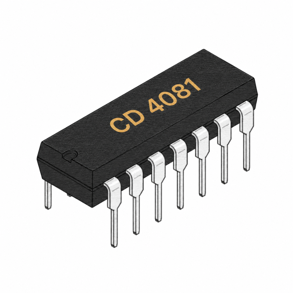
CD4031 has a supply voltage range of 5V to 20V, which is much higher than any contemporary logic family. It has buffered output which improves transfer characteristics by providing very high gain. All inputs are protected against static discharge with diodes to VDD and VSS.
CD4031 Pinout Diagram

CD4031 Pin Description
| Pin No | Pin Name | Description |
| 1 | DATA IN 2 | Data Input Pin 2 |
| 2 | CLK IN | Clock Input Pin 2 |
| 3 | NC | No Connection |
| 4 | NC | No Connection |
| 5 | Q’ | Invert Data Output |
| 6 | Q | Data Output |
| 7 | Q’ | Delayed Output |
| 8 | VSS | Supply Voltage |
| 9 | CLD | Delayed Clock Pin D |
| 10 | MODE CONTROL | Mode Control Pin |
| 11 | NC | No Connection |
| 12 | NC | No Connection |
| 13 | NC | No Connection |
| 14 | NC | No Connection |
| 15 | DATA IN | Data Input Pin |
| 16 | VDD | Drain Voltage |
CD4031 Features
- Standard TTL drive capability on Q output
- Recirculation capability
- Three cascading modes:
- Direct clocking for high-speed operation
- Delayed docking for reduoed clock drive requirements
- Additional 1/2 stage for slow clocks
- Standard Symmetrical Output Characteristics
- 100% Tested for Maximum Quiescent Current at 20V
- 5V, 10V, and 15V Parametric Ratings
- Maximum Input Current of 1μA at 18V Over Full Package Temperature Range; 100nA at 18V and +25oC
- Noise Margin (Over Full Package Temperature Range):
- 1V at VDD = 5V
- 2V at VDD = 10V
- 2.5V at VDD = 15V
| Quantity | 1 pc, 25 Pcs |
|---|
There are no reviews yet.